
 Nanooptics Group - Faculty for Chemistry and Pharmacy
Nanooptics Group - Faculty for Chemistry and Pharmacy
Nanooptics Group - Faculty for Chemistry and Pharmacy
Inorganic semiconducting nanowires are promising candidates as building blocks in nanoscale optoelectronics, photovoltaics, and sensing devices owing to their unique physical properties. In thin cadmium selenide (CdSe) nanowires (NWs), diameter-dependent quantum confinement controls the electronic band gap energy, a key parameter in potential applications. In addition, the band gap energy is known to depend on the crystal phase, since wurtzite and zinc-blende phase are stable in the nanowires. Nanoscale phase variations with alternating wurtzite and zinc-blende segments along the nanowires have been suggested as the origin of the large spectral width of the observed photoluminescence bands. The extension of TENOM as a standard technique also for inorganic nanowires would lead to a further progress in the investigation and understanding of their optical properties on nanometer length scales.
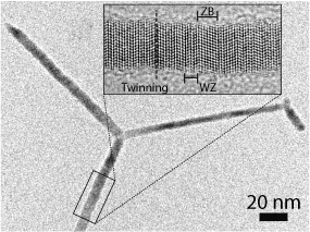
TEM image of a branched CdSe NW. Inset: HRTEM image showing crystal phase variations.